Architecture
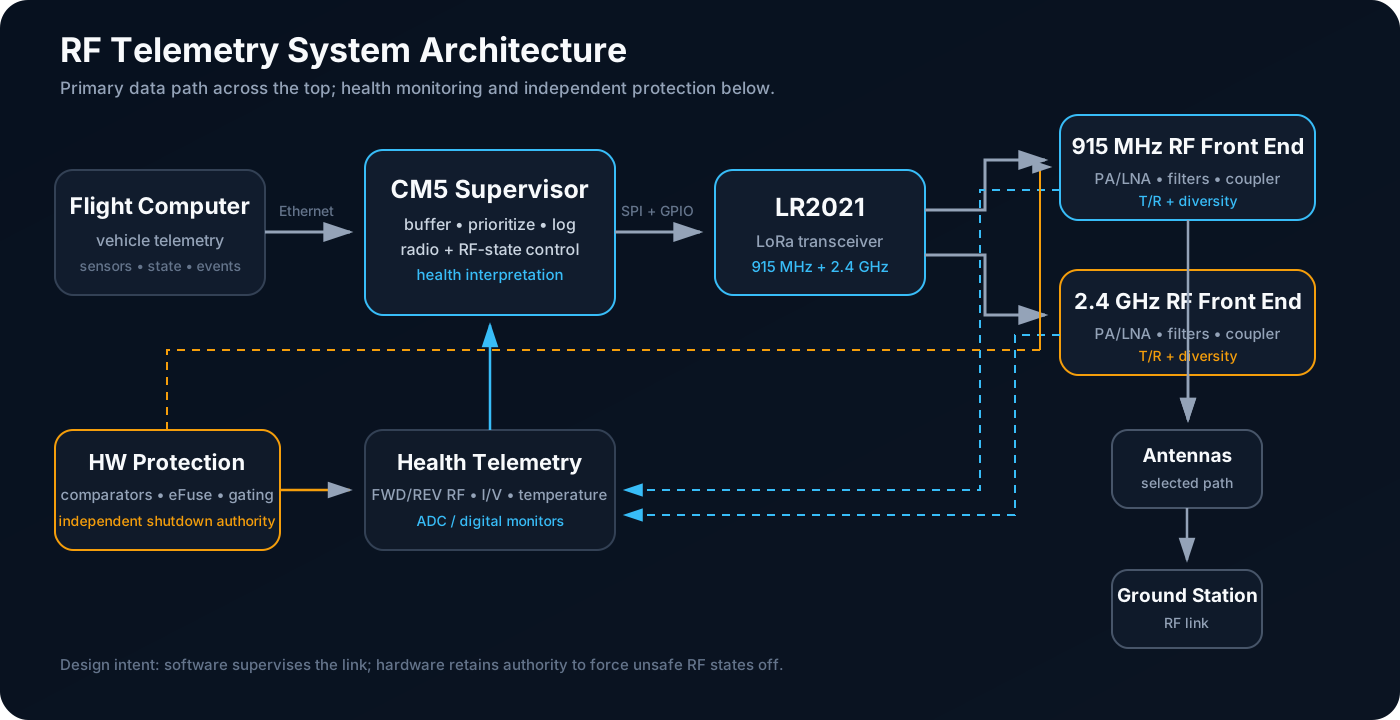
Dual-band system architecture
Current LR2021/CM5 block diagram with both RF bands, switching, detector paths, monitoring, and protection.
Dual-band LR2021 flight telemetry system for 915 MHz / 2.4 GHz with switched diversity, RF-health telemetry, and hardware fault protection
Design Responsible Engineer
Project notes
Schematics, layout, bring-up, bugs, and the decisions behind the hardware.
The reasoning, bring-up, bugs, and test results behind the board.
Project overview
915 MHz / 2.4 GHz
RF Bands
~+30.5 dBm
TX Design Target
12 channels
Power Monitors
SAFE → ACTIVE
Route Sequence
The dual-band flight radio I am currently designing around one LR2021 and a CM5. It has separate 915 MHz and 2.4 GHz PA/LNA/filter chains, switched antenna diversity, forward/reflected-power sensing, twelve power-monitor channels, and hardware that can shut the RF side down without waiting on Linux.
Still in design. The architecture, power budget, fault tree, and routing state machine are defined, but the RF numbers stay as targets until Rev 1 is built and measured.
Hardware & test evidence
Architecture
Current LR2021/CM5 block diagram with both RF bands, switching, detector paths, monitoring, and protection.
Design artifact
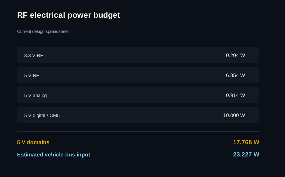
Current design budget: about 17.77 W on the 5 V domains and about 23.23 W estimated at the vehicle bus.
Design artifact
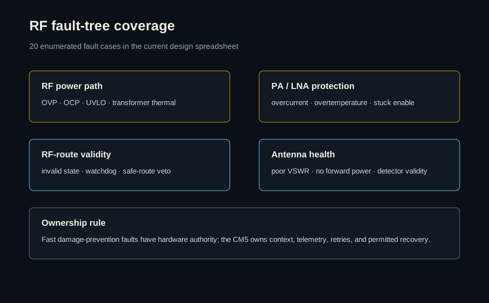
Twenty explicit fault cases covering PA/LNA thermal faults, RF power, mismatch, routing states, watchdogs, and bad measurement data.
Test history
Rev 1 flight telemetry
Designed
Current LR2021/CM5 flight-radio architecture. Schematic/layout work and all hardware validation are still in progress.
Design deep dives
Architecture
Ethernet → SPIHow flight data gets into the radio, what the CM5 owns, and where the hardware protection sits outside the software path.
RF
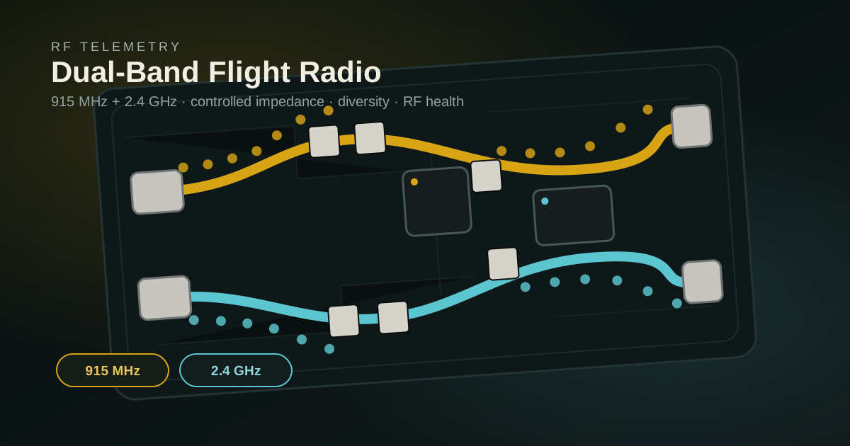
915 / 2.4 GHzThe 915 MHz and 2.4 GHz TX/RX chains, switching sequence, diversity, filtering, and the layout rules I am designing around.
Telemetry
FWD / REVHow I plan to measure forward/reflected RF power, digitize it, calibrate it, and avoid pretending the coupler gives perfect VSWR.
Safety
HW shutdownHow current, temperature, RF mismatch, illegal switch states, and software failures map into hardware shutdown versus software recovery.