Dual-Band RF Path
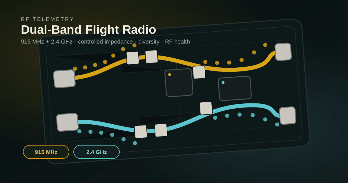
The LR2021 can handle both bands, but I still split the external RF front end into separate 915 MHz and 2.4 GHz gain/filter/routing chains. Only one band and one direction are allowed to be active at a time.
Functional TX Chain
| Stage | 915 MHz path | 2.4 GHz path | Design intent |
|---|---|---|---|
| Radio | LR2021 LF output | LR2021 HF output | Generate the commanded LoRa waveform |
| Gain | External PA | External PA | Raise radio output toward the approximately 1 W system target |
| Harmonic filtering | Band-specific LPF | Band-specific LPF | Reduce PA-generated harmonics before the antenna network |
| RF sensing | Directional coupler | Directional coupler | Sample forward/reflected traveling waves |
| T/R + diversity | RF switch network | RF switch network | Select direction and antenna path |
| Radiation | 915 MHz antenna | 2.4 GHz antenna | Send the selected band to the ground station |
The ~1 W number is a system target, not 'the PA datasheet says 1 W so we're done.' Final LR2021 drive, PA compression, filter loss, coupler loss, switch loss, trace loss, and connector loss must be measured together before the antenna-port power is considered verified.
Functional RX Chain
| Stage | Function |
|---|---|
| Antenna/diversity selection | Choose the desired physical antenna path |
| T/R switch | Disconnect the TX chain and route the antenna toward the receiver |
| LNA | Improve weak-signal level before subsequent loss |
| Band-pass filter | Reject out-of-band interference before the LR2021 input |
| LR2021 | Demodulate the selected 915 MHz or 2.4 GHz signal |
A big LNA gain number by itself does not tell me much. I still have to care about NF, filter/switch loss, blocker handling, compression, and how much garbage the CM5/power converters spray into the receive side.
Why Half-Duplex Switching
Switching Invariant
I am treating the RF switches like a state machine, not a bag of GPIOs that software can flip in any order.
| Step | Required action |
|---|---|
| 1 | Disable the active PA and LNA |
| 2 | Allow RF output to decay |
| 3 | Change T/R and/or antenna-selection switches |
| 4 | Wait for switch settling |
| 5 | Enable only the amplifier needed by the new state |
| 6 | Begin transmit or receive operation |
The whole point is to make it hard to hot-switch a live PA or accidentally dump RF into a bad/unknown path.
Diversity
The antenna switch network is intended to give the CM5 a second path when the selected antenna is poorly matched or the link quality degrades. Diversity only helps if I can tell 'bad antenna/path' from 'the PA or radio is the thing that's broken'; this is one reason forward/reflected RF telemetry is part of the architecture.
PCB Requirements
- Controlled-impedance routing from the LR2021 through switches, filters, couplers, and connectors
- Continuous RF return paths with no accidental plane gaps beneath critical transmission lines
- Via fencing and compact ground-return geometry around RF launches and switching nodes
- Physical separation between sensitive RX regions and CM5/Ethernet/switching-power noise sources
- Short, low-inductance decoupling around PAs, LNAs, switches, and the LR2021
- Thermal copper and via structures sized around PA dissipation rather than RF routing alone
- Layout access that still permits VNA, spectrum-analyzer, and conducted-power validation
Open RF Items
- Final PA/LNA/filter selections for both bands
- Measured PA gain/compression versus LR2021 drive setting
- Final T/R and diversity switch insertion loss, isolation, and power handling
- Antenna-port conducted-power target after all downstream losses
- Receiver cascaded noise figure and blocker tolerance
- Final controlled-impedance geometry from the production stackup