Recovery System Engineering Notes
Purpose
Recovery is the board that decides when the rocket is actually allowed to deploy the parachutes. It packs redundant compute, hardware voting, safing, local sensing, protected power conversion, and ten high-current ignition channels onto one six-layer PCB.
The tricky part is that firing an output is only half the job. The board also has to stay safely inhibited during integration, survive a single control-domain fault, handle all ten channels firing at once, and keep the MCUs and sensors alive through the resulting load dump when those loads turn off.
My Responsibility
I was the Design Responsible Engineer for the board. I owned the architecture, schematic, PCB layout, reviews, bring-up, debugging, validation, and the day-to-day hardware support after it was built.
Architecture
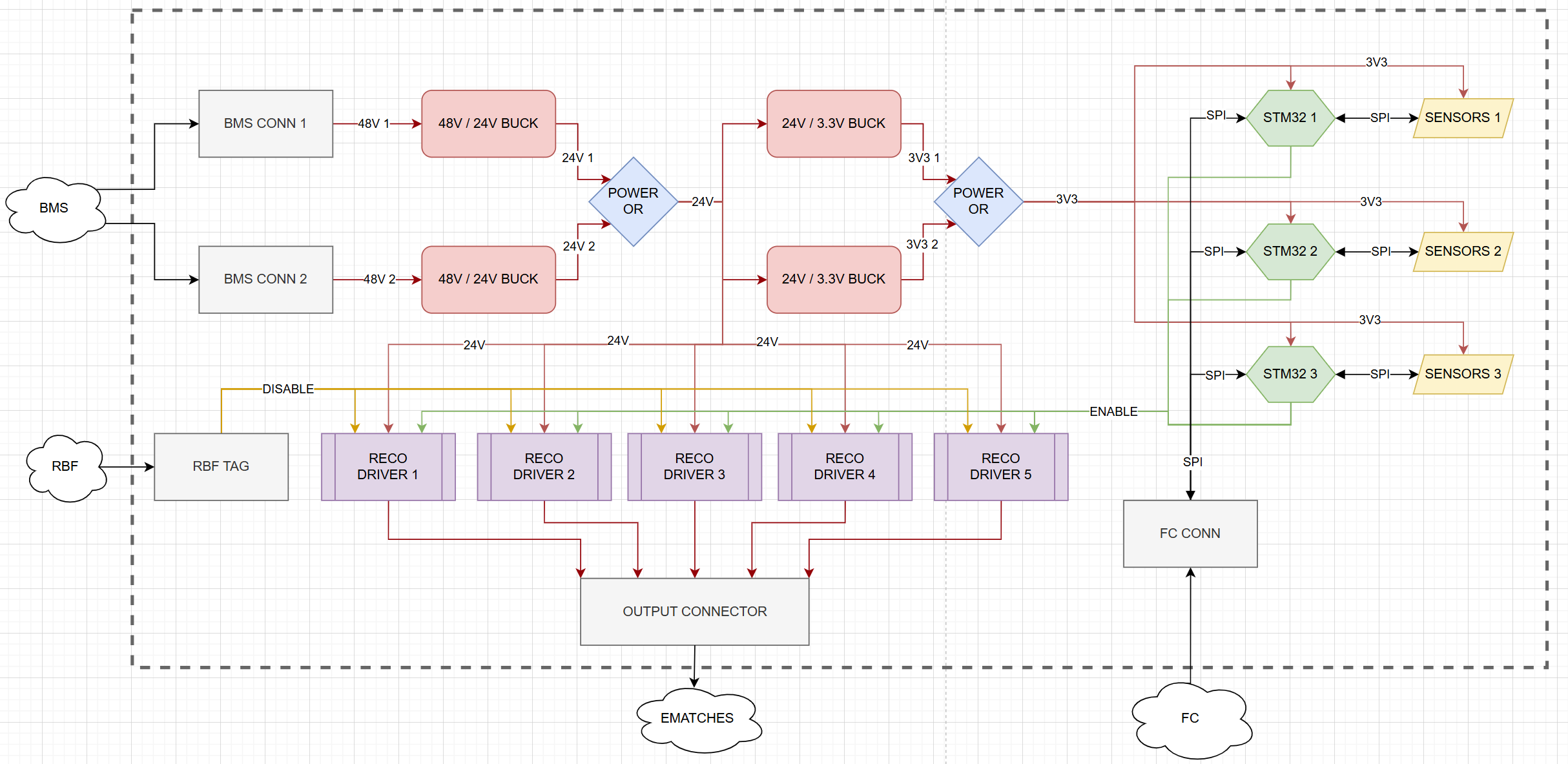
There are two protected battery feeds, and I keep them separate through the power tree before they reach the parts of the design that are intentionally shared. Four buck converters generate the 24 V deployment rails and 3.3 V logic rails.
Three STM32 domains each process their own local sensor data and receive flight-computer commands. Their deployment decisions do not go straight to the drivers; they first pass through discrete median-voting logic. RBF, ESTOP, abort, and software-enable paths add a few more independent ways to keep the deployment hardware off when it should be off.
Ten output channels handle the actual 24 V deployment loads.
Power Architecture
The two input paths stay independent through the protected-input and regulation stages so one upstream fault does not quietly take down both sides of the recovery system.
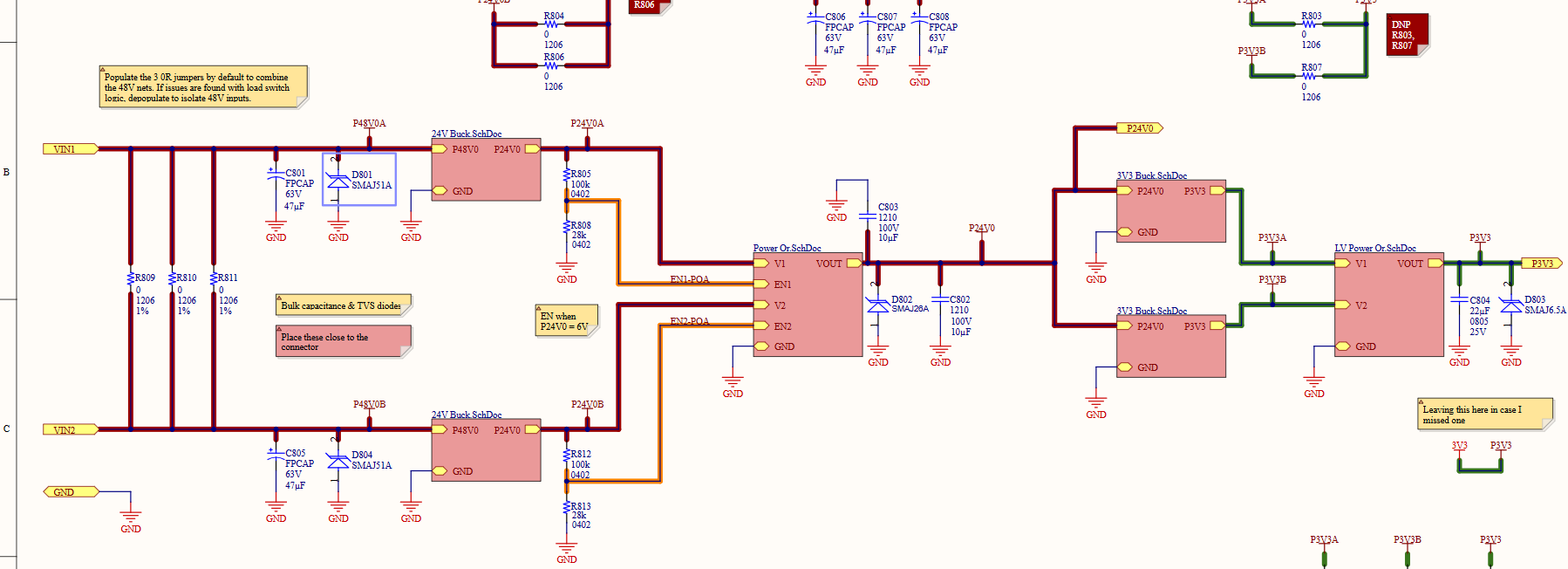
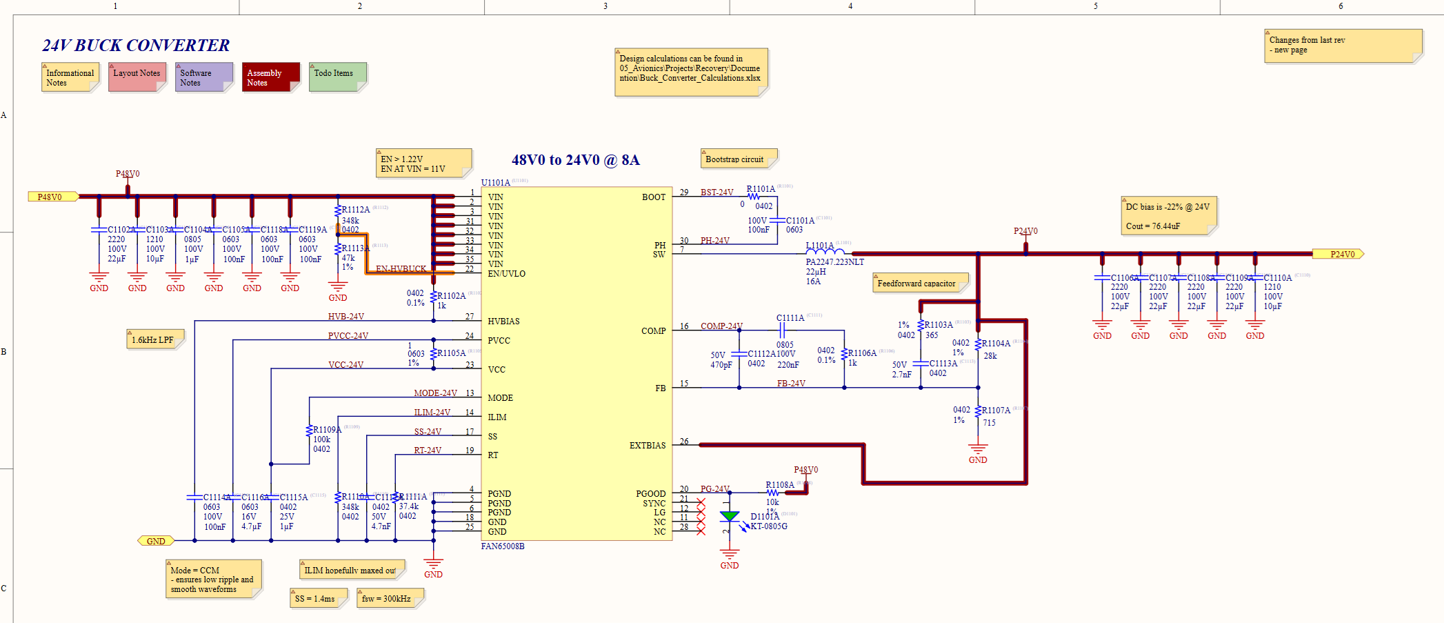
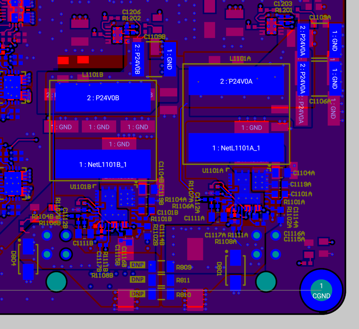
The 48 V → 24 V converters feed the deployment rails, and they ended up being the part I cared about most during the worst-case load-dump testing.
Fault-Tolerant Control
One MCU is never enough to directly authorize deployment. The three command paths stay separate until the voter, and the hardware safing chain can still block the deployment path even if the software state is wrong.
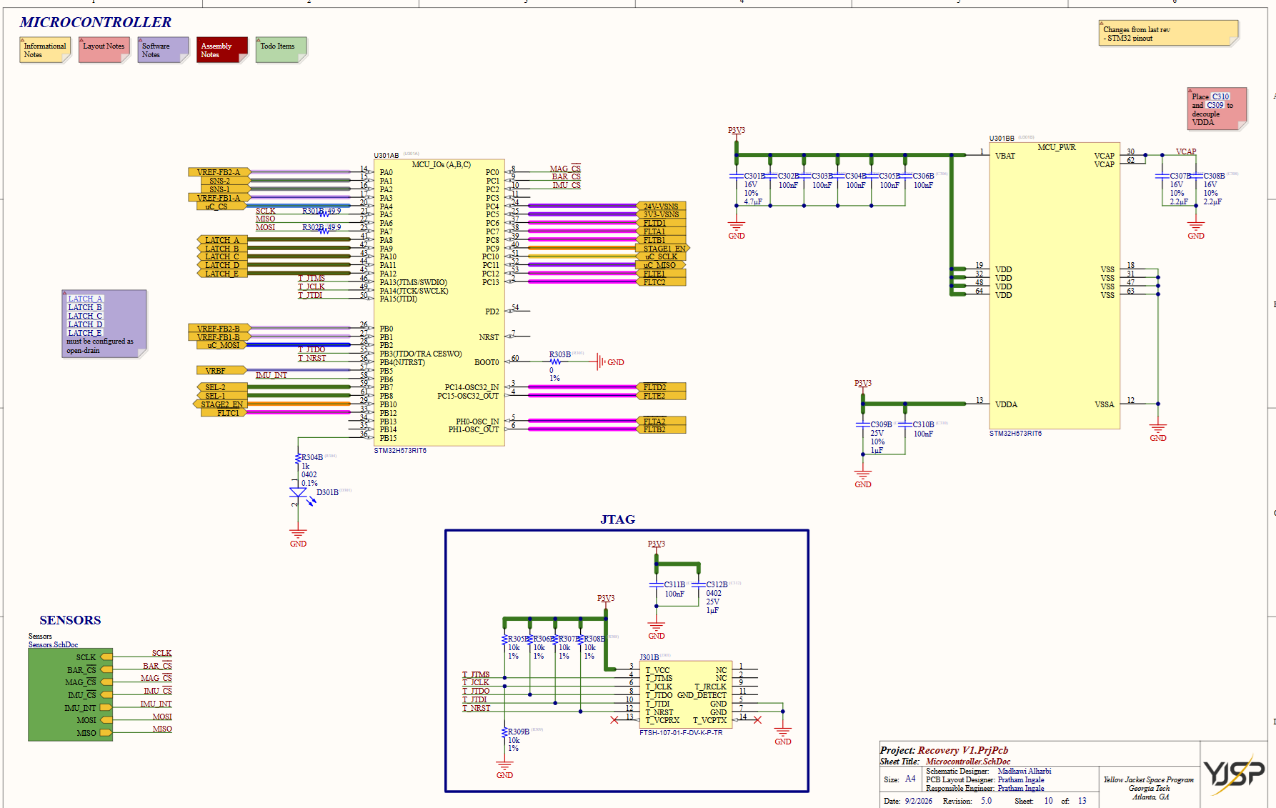
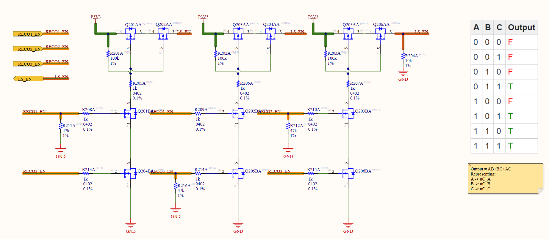
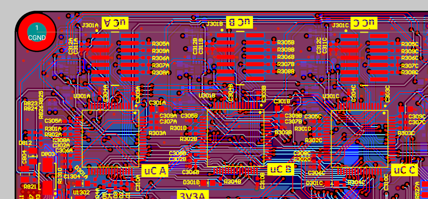
I tried to carry the same separation into the PCB. Signals from different control domains stay physically separate where practical, and they only come together where the architecture actually requires it.
Ignition Drivers
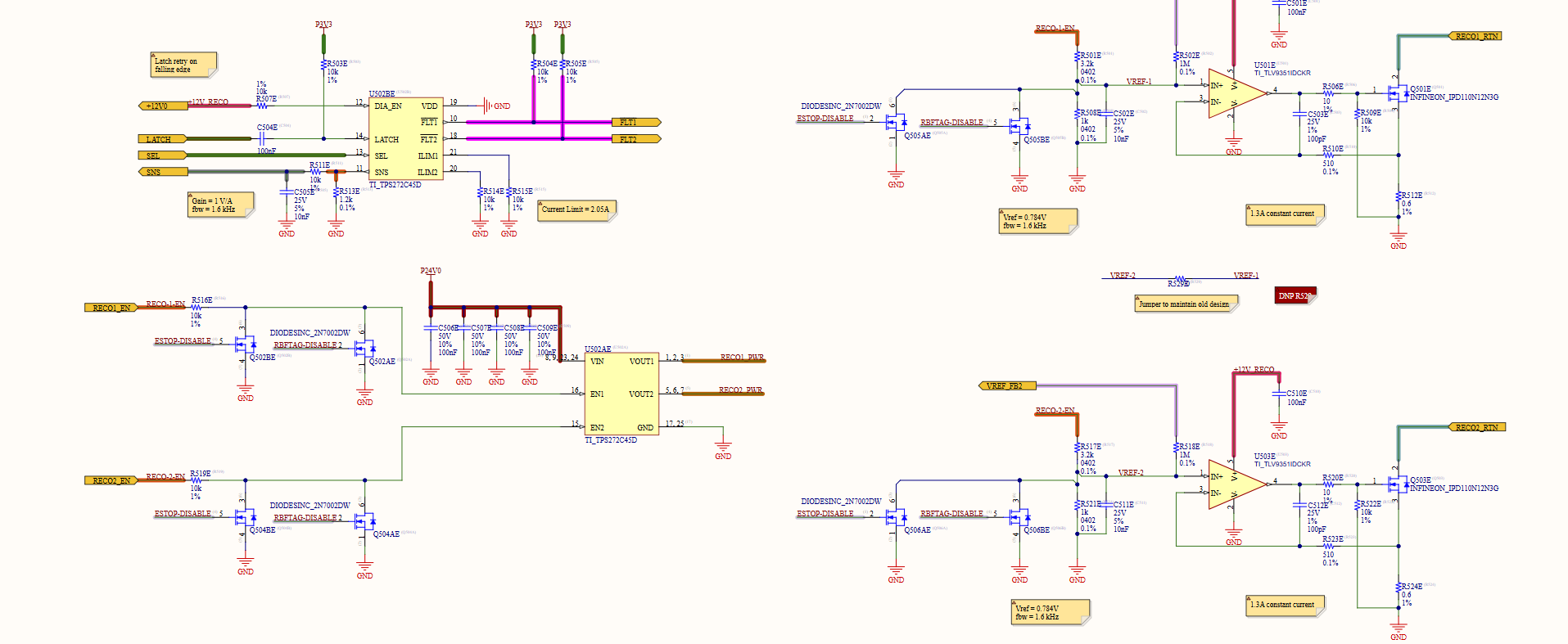
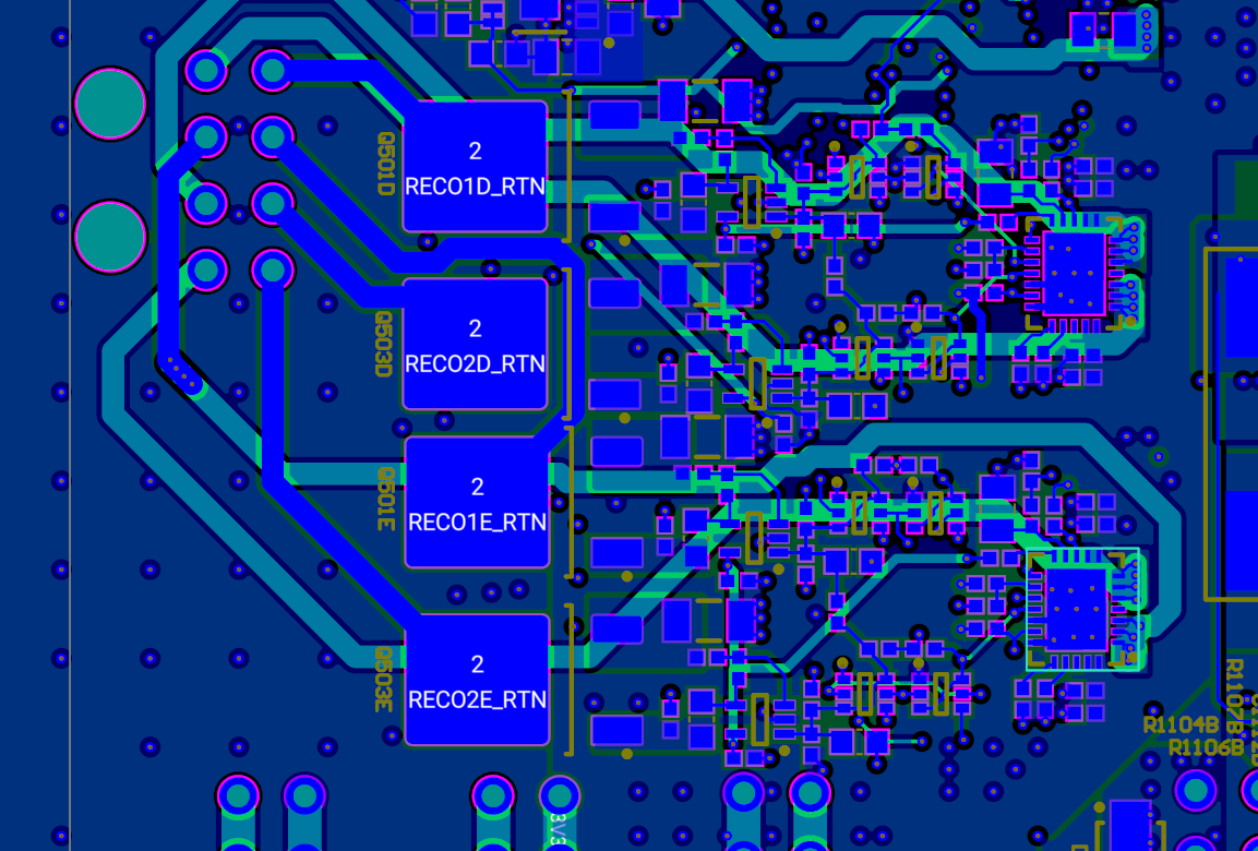
Each deployment output is a current-controlled 24 V channel with command, current sensing, and fault feedback. Since there are ten copies, consistency mattered a lot: the layout, current path, and control behavior had to look and behave the same across the bank.
PCB Layout
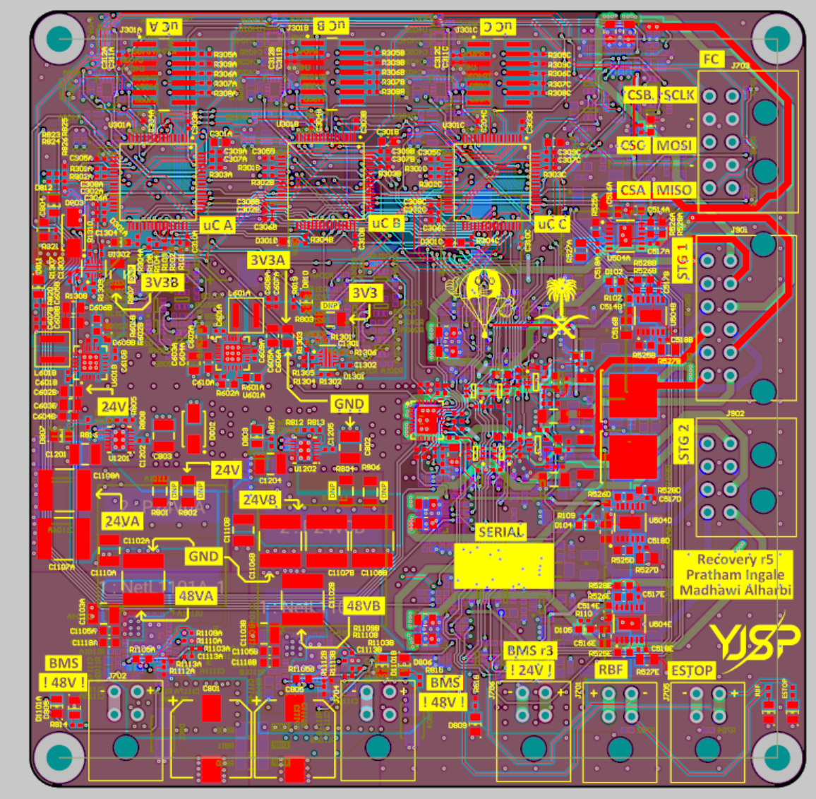
The layout problem I cared about most was the current path during deployment. I kept the switching devices, output connectors, bulk capacitance, and returns close enough that the high-current loop did not have to wander across the board.
The low-level sensing, MCU, and voting circuitry stay away from the driver banks and switching nodes. The six-layer stackup gives me two ground-reference layers, one power layer, and three signal layers to keep those current paths and references reasonably clean.
Bring-Up and Validation
I brought the board up in layers: power paths first, then regulated rails, MCU communication, sensors, voting, safing inputs, individual outputs, and finally the full deployment case.
The hardest test fired all ten e-match loads at once. While active they drew roughly 300 W; the problematic event was turn-off, when all ten loads dropped out together and the load collapsed from about 300 W → 0 W. On the first run, that load dump drove the 3.3 V rail to 8.2 V and the 24 V rail to 32.5 V.
The drivers themselves were not the problem. The upstream 48 V → 24 V converter was responding too slowly. I changed the compensation from a 22.6 kHz crossover to 49.7 kHz and reran the same test. The 3.3 V peak dropped to 3.9 V and the 24 V peak dropped to 26.9 V, which got rid of the MCU overvoltage condition.
RBF hot-plug transient
The main power bring-up had actually gone pretty smoothly. I checked the rails and power ORing and loaded the 24 V output to about 9.5 A as a steady-state check. After fixing the converter compensation, I repeated the ~300 W → 0 W load-dump test and then ran the same load-dump check with Recovery powered through the BMS. The BMS/load-switch path stayed up through the event.
The more annoying failure showed up later on the much smaller RBF interface.
The first RBF test looked completely normal: I powered the board with the tag installed, removed it and saw the board disable correctly, then plugged it back in. That second hot-plug created a transient large enough to kill one STM32.
I shut the supply down immediately, removed the damaged MCU, and checked that the rest of the board was not shorted. I also changed the test plan instead of risking another populated board: Reco-51 stayed available for software bring-up, while I moved the RBF hardware debugging onto Reco-52.
The next day, Reco-51 was still healthy enough for the software team to connect to all three STM32s, talk to the sensors, and verify the ADC readings. On Reco-52 I worked the RBF issue separately and ended up with a simple series-damping fix.
I had not put a resistor footprint in that connector path, so the Rev 5 rework was about as literal as it gets: I cut the connector pins and soldered the resistor inline.
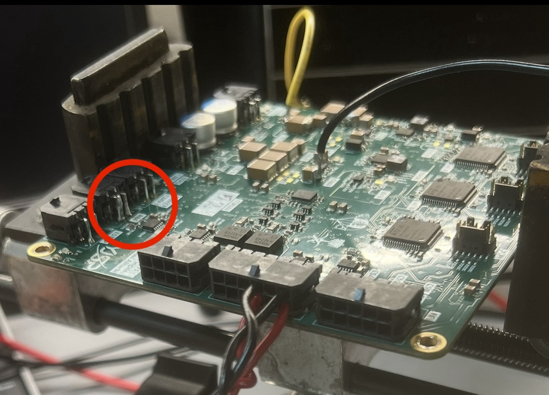
The important part for the next revision is not “copy the bodge.” It is to give this interface a proper place for damping and make full-length-harness hot-plug testing part of normal bring-up. There is not a Rev 6 board yet; those changes are only in my next-revision notes right now.
Key Result
After the compensation change, all ten deployment channels could fire together without resetting or overstressing the downstream control electronics.
Next Revision
For another revision, I would add better high-bandwidth rail-monitoring test points, clean up a few shared-support areas between redundant domains, and fold the exact validation setup into the production test docs.