Dual-Tree Power Architecture
Recovery has two jobs that fight each other a little: stay fault tolerant like a safety system, but also dump a lot of power into the deployment loads for a short time. So I treated the power tree as part of the redundancy architecture instead of one shared utility rail.
Architecture
Two protected battery feeds enter separate power trees before the design converges at the intentionally shared deployment circuitry. Four conversion stages generate the 24 V deployment and 3.3 V logic domains used by the redundant control paths.
The rules I designed around were pretty simple:
- a fault in one local control/power domain should not quietly disable every controller;
- the logic rails must remain alive while multiple deployment channels switch at once;
- high-current return paths must not become the reference path for sensors or voting logic;
- hardware safing must remain deterministic regardless of software state.
The six-layer stackup supports that partitioning with two ground-reference layers, a dedicated power layer, and three signal/component layers.
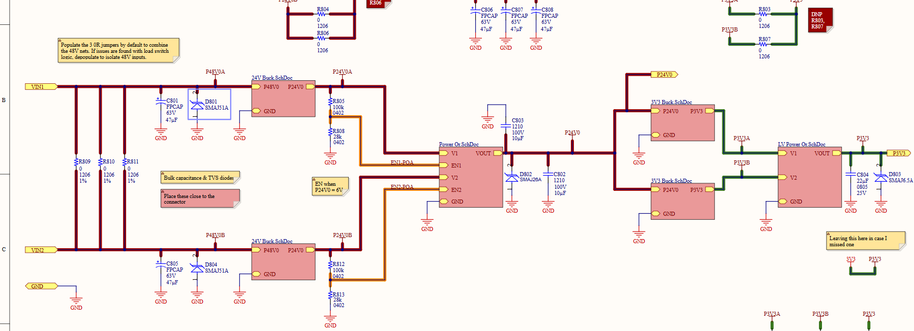
Distribution and Layout
The deployment bank creates the dominant dynamic load event. I kept the converter loops compact, used low-impedance distribution into the driver region, and treated the high-current output/return paths as a separate physical region from MCU and sensor circuitry.
The layout question I cared about was not just “is the copper wide enough?” It was whether that current could get from the converter/bulk caps to the deployment bank and back without dragging the low-voltage control reference along for the ride.
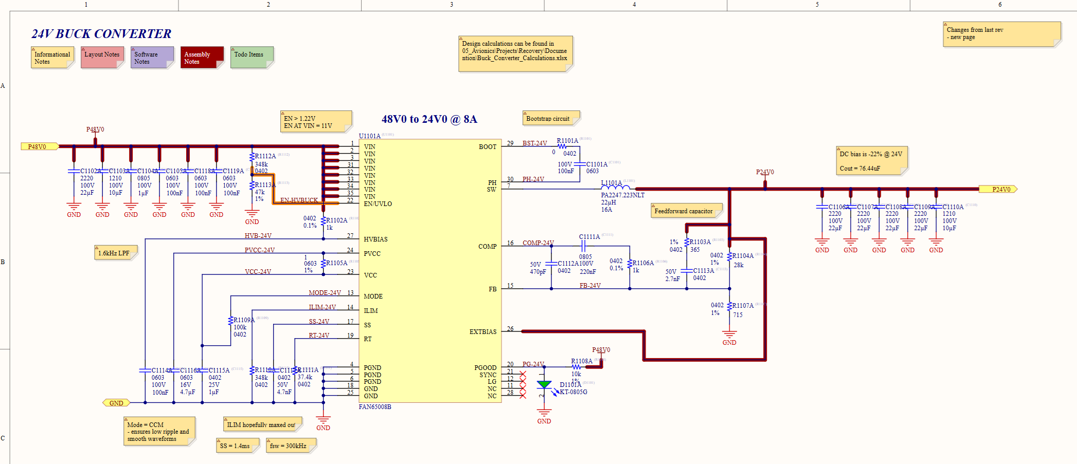
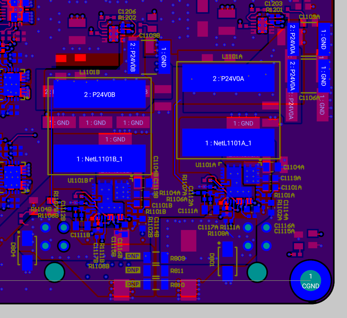
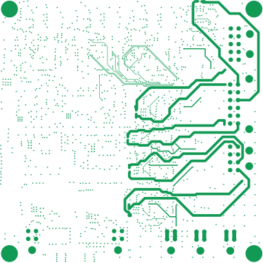
What Bring-Up Exposed
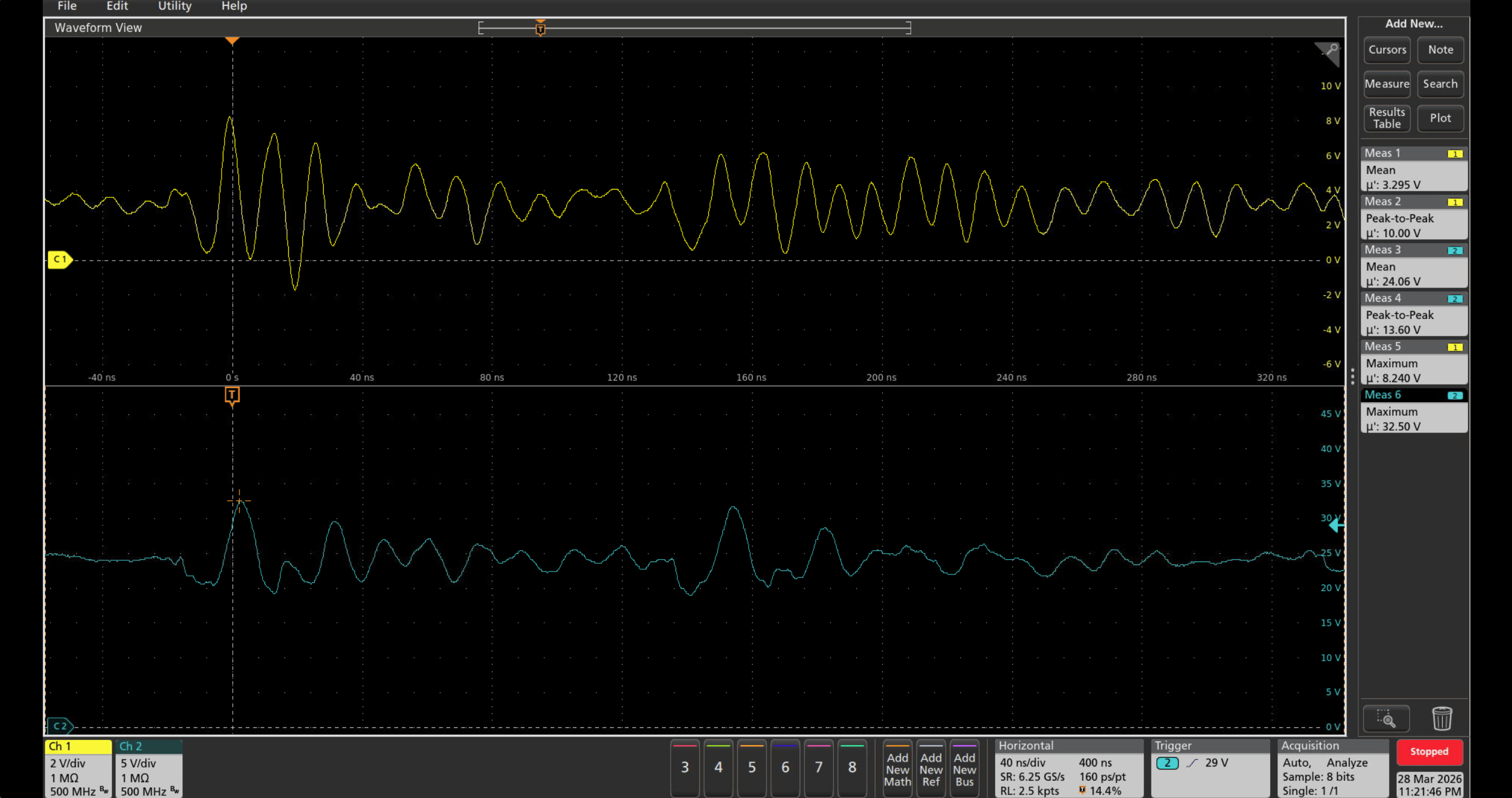
The first full simultaneous-deployment test fired ten e-match loads at once. While active, the bank drew approximately 300 W. The failure appeared at turn-off, when all ten loads switched off together and the load dropped from about 300 W → 0 W. The upstream 48 V → 24 V converter responded too slowly to that load dump: the 24 V rail peaked at 32.5 V, and the downstream 3.3 V rail reached 8.2 V—high enough to create an MCU overvoltage condition.
That failure was actually helpful because it told me the driver bank was not the problem. The load path was doing its job; the converter loop just was not reacting fast enough.
Compensation Change
I changed the compensation capacitor from 220 nF to 100 nF, moving the calculated crossover frequency from 22.6 kHz to 49.7 kHz, then repeated the same 300 W → 0 W load-dump event.
3.3 V peak during 300 W → 0 W load dump
Before
8.2 V
After
3.9 V
The 24 V rail peak simultaneously improved from 32.5 V to 26.9 V.
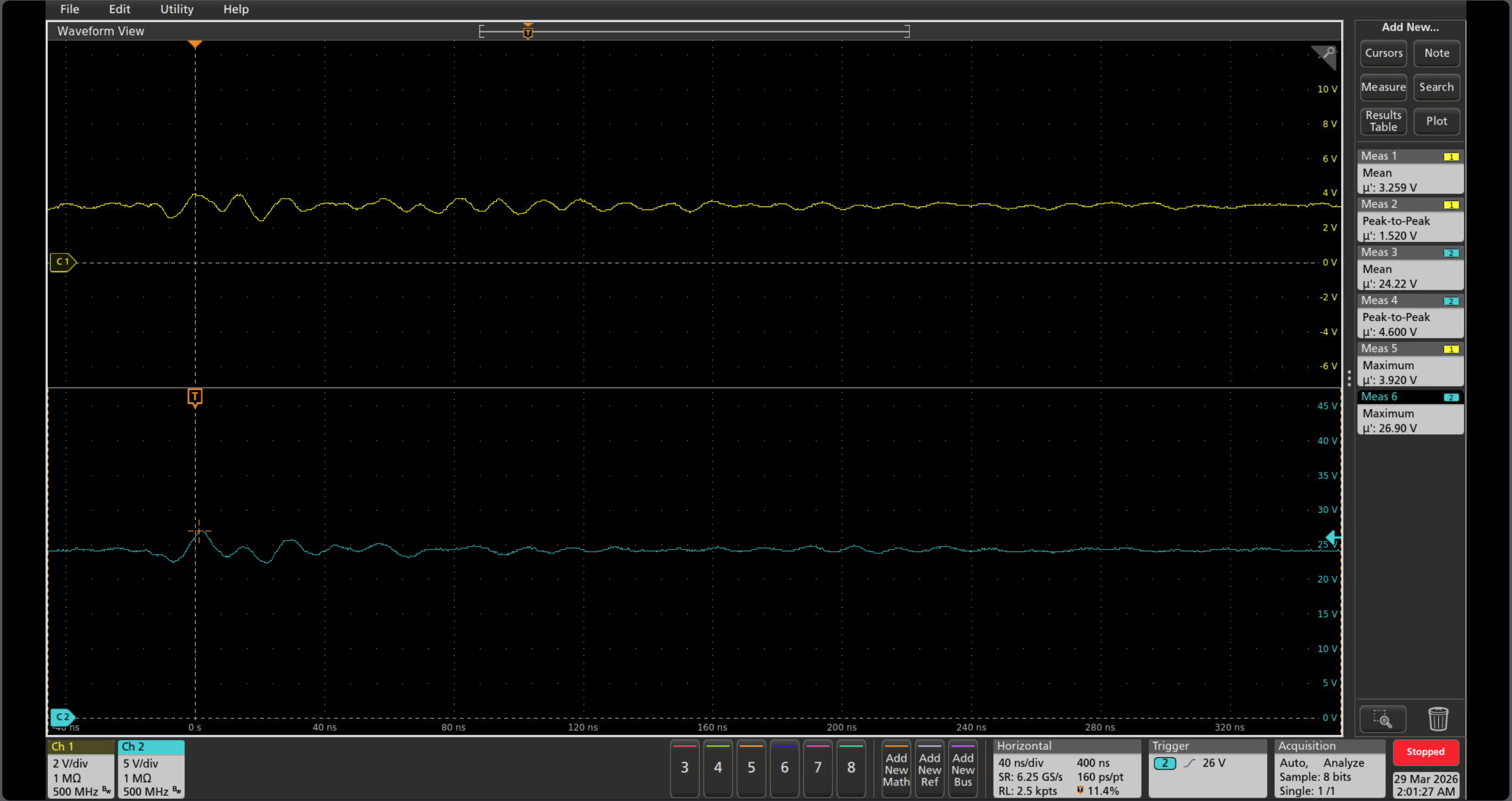
After the compensation change, all ten channels could operate together without the downstream MCU overvoltage/reset condition.
Characterization
I also swept the external 24 V load during bring-up. Measured external-load efficiency peaked at 95.62% at 144 W output.
<Figure src="/generated/recovery-system/evidence/power-characterization.svg" alt="Recovery 24 V power characterization" caption="Measured external-load efficiency sweep from the Recovery power-stage bring-up." /> Because the calculation excludes the board's internal 24 V consumption, I present it as an external-load efficiency measurement rather than a complete converter-loss model.