Ignition Driver Channels
Rev 5 has ten 24 V deployment outputs. This is the point where tiny logic signals turn into a pretty aggressive current event, so I treated the driver bank like its own subsystem instead of ten copies of a GPIO-controlled switch.
Channel Structure
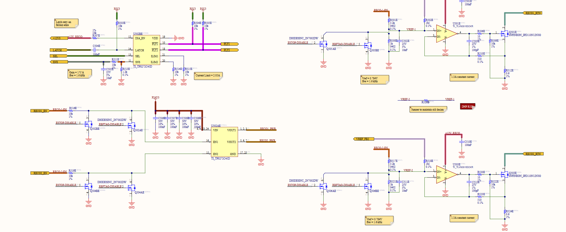
Each channel sits behind the board-wide safing/voted-enable chain and includes the switching/current-control path required to drive the external deployment load. The channels are replicated so command behavior, sensing, and fault handling stay consistent across the bank.
The useful design boundary is:
controller decision → hardware vote / safing → channel command → power switch → deployment load
No individual MCU GPIO directly owns the high-current output.
Disabled-State Behavior
For a recovery driver, the most important state is honestly the off state. During assembly, integration, and vehicle handling, live energetic devices may eventually be connected to the harness, so the design needs multiple reasons to remain disabled before it needs one reason to fire.
The hardware safing path therefore stays upstream of the individual channel commands. A channel cannot become active simply because its local command line changes state.
High-Current Layout
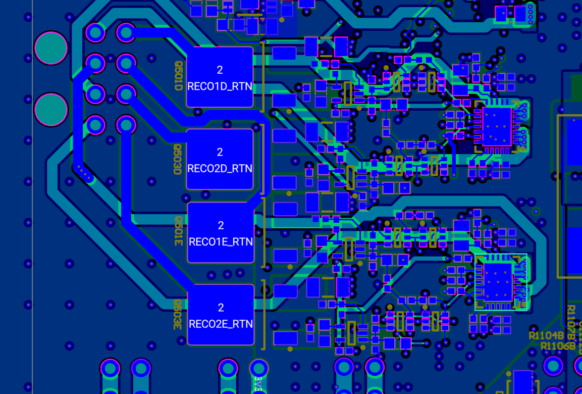
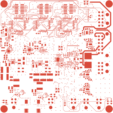
All ten channels sit in a deliberate high-current region of the board. The routing priorities were:
- short output paths from the switched power region to the connectors;
- short, low-impedance return paths;
- bulk capacitance close enough to support the event rather than forcing every edge through a long distribution path;
- gate/control routing kept away from the highest-
di/dtcopper; - sensor/MCU references kept out of the deployment return path.
The Multi-Channel Problem
One channel working on a bench supply is easy. The interesting case is all ten changing the source current at basically the same time.
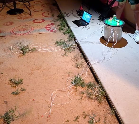
That is why the final test fired ten e-match loads simultaneously. The bank drew approximately 300 W while active, and the worst-case event came at turn-off when all ten loads switched off together, producing a ~300 W → 0 W load dump.
Validation Philosophy
I brought the driver bank up from the inside out: safe-state logic first, individual outputs next, then the full ten-channel event. That way a command-path bug and a power-distribution bug do not get mixed together during debugging.